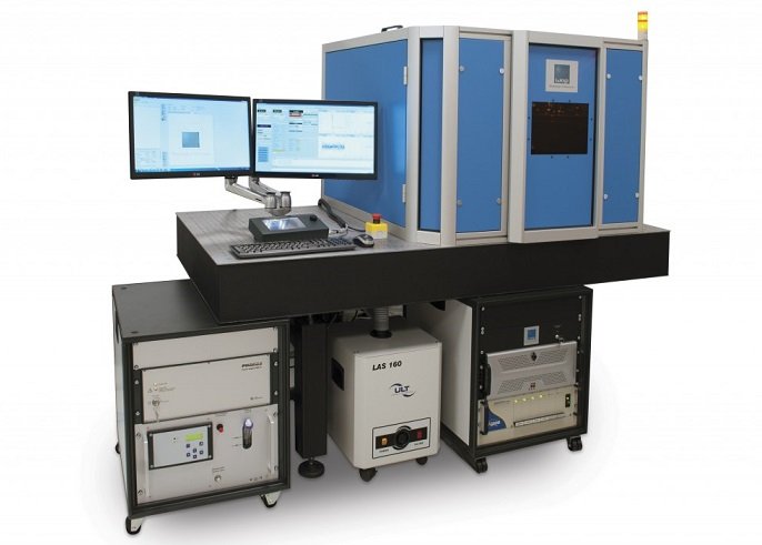
Femtosecond Laser Micro/Nano Processing System
Brand
WOP
Model
FemtoLAB
Place of origin
立陶宛
Location
E3-129
Main specifications
1. Center Wavelength: 1030 nm ± 10 nm;
2. Pulse Width: Adjustable from 290 fs to 10 ps;
3. Repetition Rate: Single pulse up to 1 MHz;
4. Maximum Output Power: 6 W;
5. Maximum Single-Pulse Energy: 100 μJ @ 1030 nm;
6. Beam Shaping: Switchable between Gaussian, annular (ring-shaped), and vortex beams;
7. Positioning Stage: XYZ total travel range 160 mm × 160 mm × 50 mm;
8. Microscope Objective: 20X, 0.4 NA, working wavelength range 480–1800 nm;
9. Sample Holder: 100 × 100 mm;
10. High-Damage-Threshold Diffractive Optical Elements (DOEs):
Damage threshold > 63 J/cm² @ 1064 nm, 10 ns pulse
Damage threshold > 2 J/cm² @ 1030 nm, 212 fs pulse;
11. Laser Microprocessing Control Software (SCA – System Control Application): Modular architecture for seamless integration and control of various hardware components
Main functions
- The system integrates a high-performance femtosecond laser, precision linear positioning stages, a high-reliability galvanometer scanning system, and advanced processing software. It delivers sub-micron resolution machining capabilities and supports customized development for diverse processing tasks;
- The platform exhibits excellent material compatibility, including but not limited to: glass, sapphire, silicon, ceramics, metals, polymers, and optical fibers;
- The system enables design and simulation of integrated photonic devices, optical waveguides, and specialty fibers. It facilitates research on novel photonic device characteristics, providing theoretical guidance and data support for subsequent fabrication processes;
- Key Applications:
Surface and volume micro- and nano- structuring
Femtosecond laser ablation(FSLA)
Laser grooving
Multiphoton polymerization (MPP)| direct laser writing (DLW)
Laser cutting & drilling Micromachining on optical fibers